Winbond W25N02KVxxIR/U
The Winbond W25Nxx memory IC series uses NAND flash where the Winbond W25Qxx series (and many compatible devices from other vendors) uses NOR flash. Despite this, the W25Nxx series uses a command set that seems compatible with the W25Qxx NOR flash command set... until you look closer.
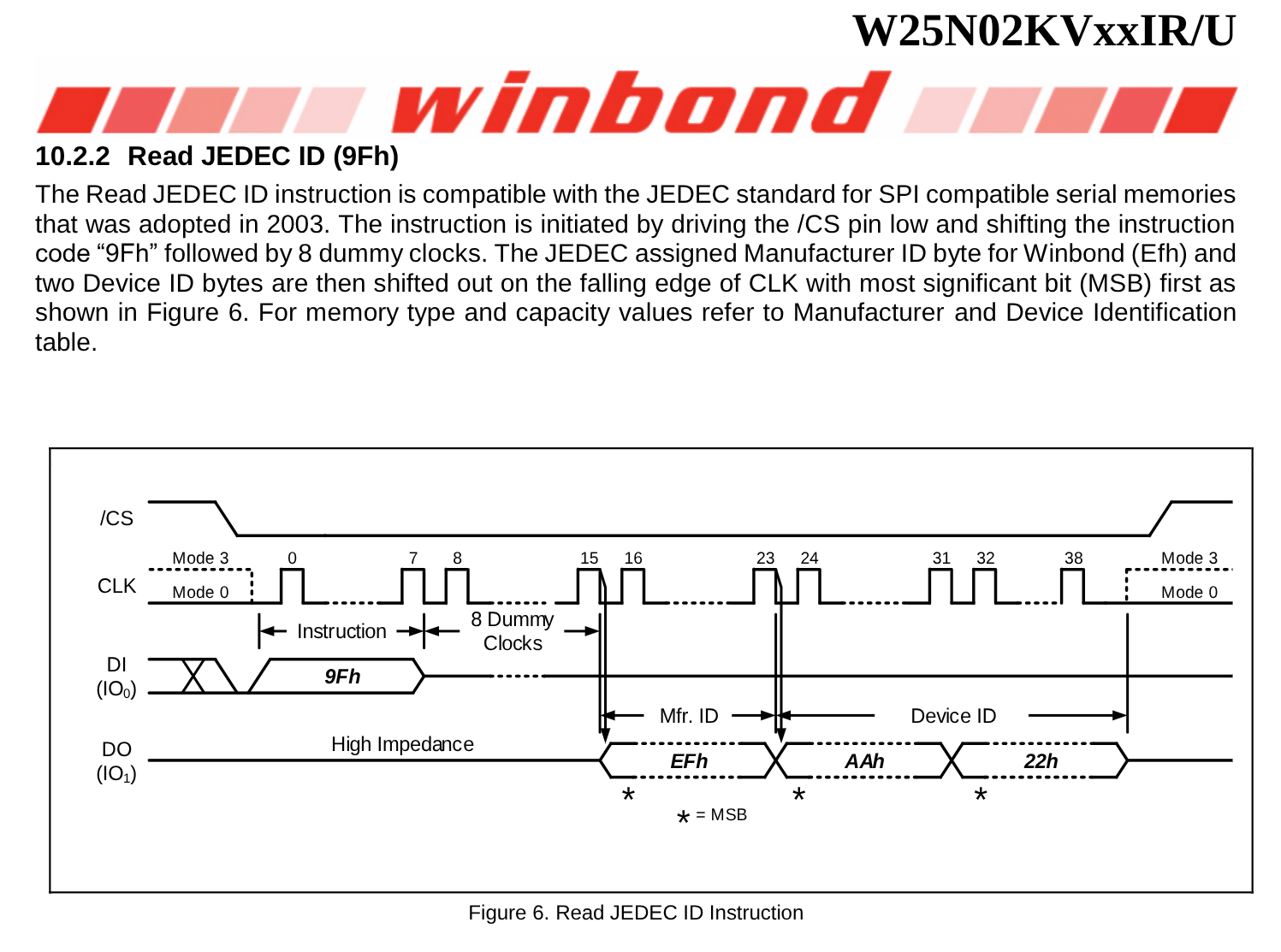
The 9Fh JEDEC ID command in any other SPI flash, from any manufacturer (including Winbond), is followed by MF7:0 then ID15:0 immediately. This flash requires 8 dummy clocks first, making sure no existing SPI flash firmware can even identify it correctly or meaningfully:
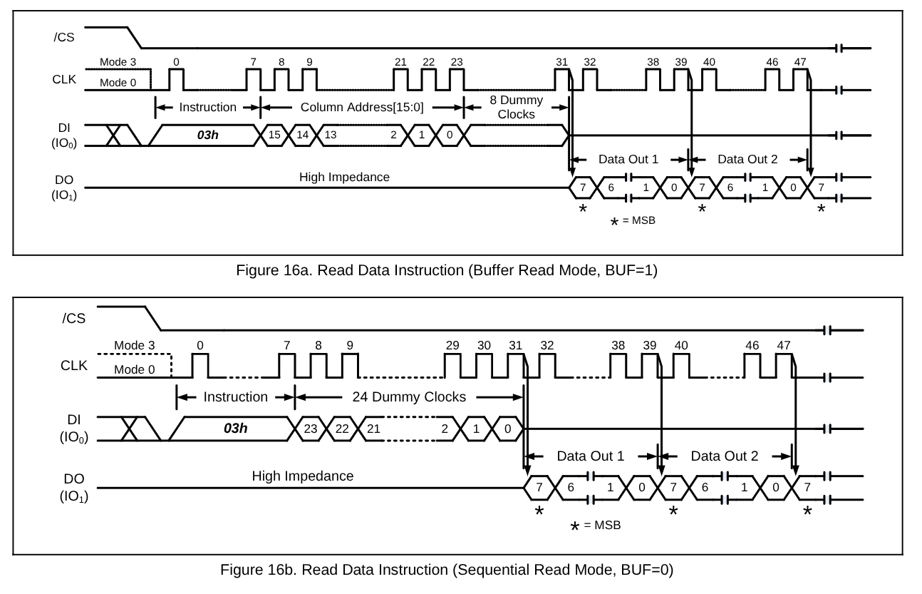
The 03h Read command works more or less how you'd expect (except for the addressing, but one can excuse that):
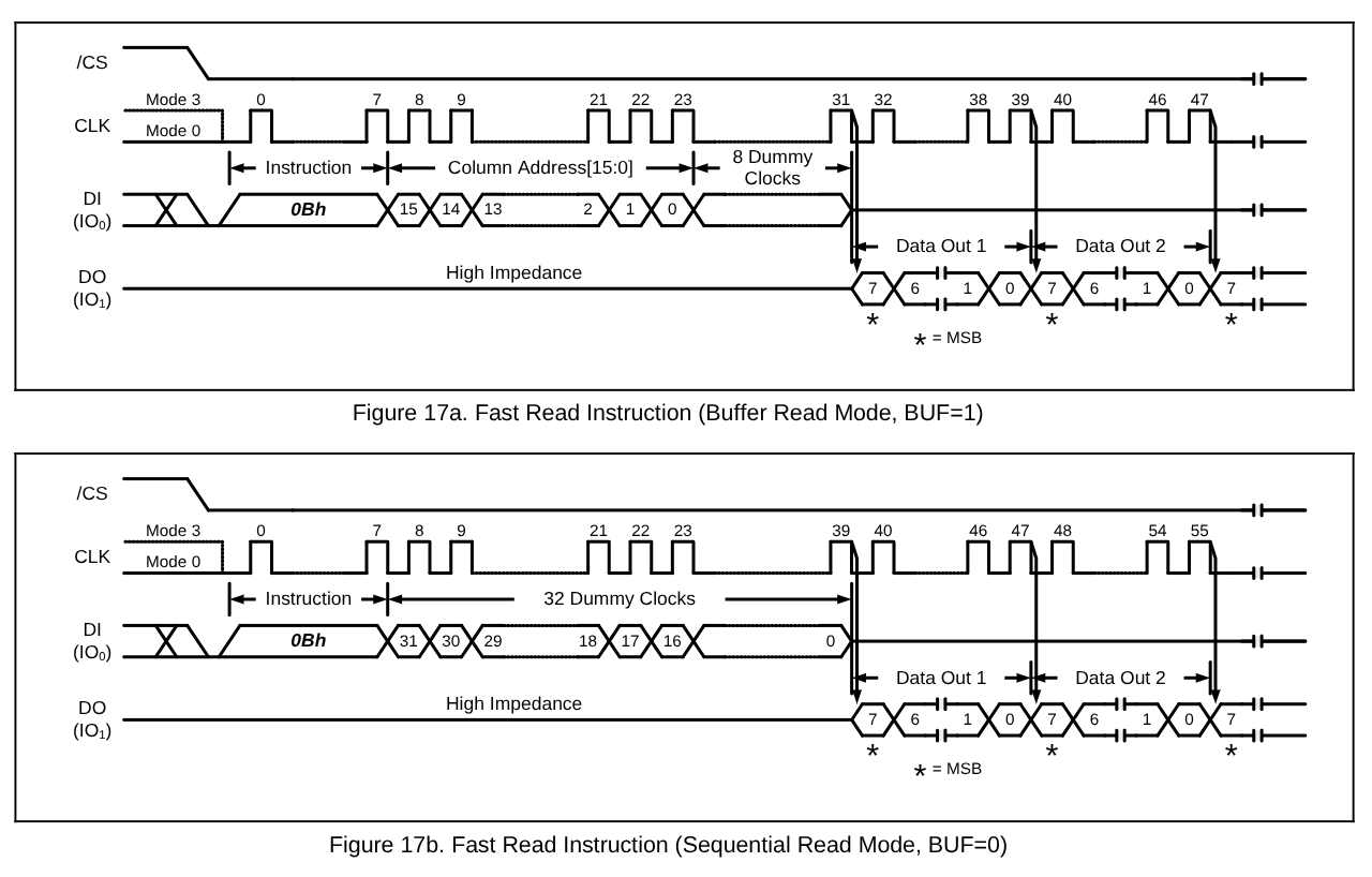
The 0Bh Fast Read command, which in NOR flash command set accepts an address and 8 dummy clocks (these dummy clocks being its entire reason for existing separately from 03h Read), in this device, sometimes has 8 more dummy clocks, depending on BUF mode bit:
Also, even though the device has "enable internal ECC" mode, and "read out the entire device sequentially" command, these two cannot be used together; if you want to use it with a device that understands the NOR command set only and configures using a single long 0Bh Fast Read command (e.g. any FPGA, some MCUs) you're out of luck.
What was the point of maintaining an appearance of compatibility?